JTAG Manager - DCC Read/Write TAB
This manual describes RIFF JTAG Manager - DCC Read/Write TAB, devided into sections:
- DCC Read/Write TAB Functions and buttons description
- How to read full flash from target device
- How to write full flash to target device
- How to erase full flash on target device
RIFF JTAG Manager DCC Read/Write TAB Functions and buttons description:
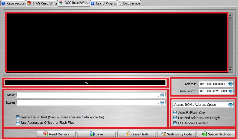
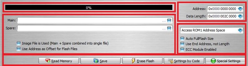
As You can see, DCC Read/Write TAB inerface is devided into few sections:
- Logging Window section (No additional description required)
- Progress bar section (No additional description required)
- File(s) openining and options section
- Address and Data Length section
- Target Device Address Space options section
- Function buttons section
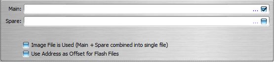
Main data file field:
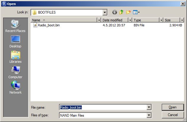
Used for all flash memory types. (NAND, NOR, eMMC) To open file, tick the check box and click "..." which will bring file open dialog.
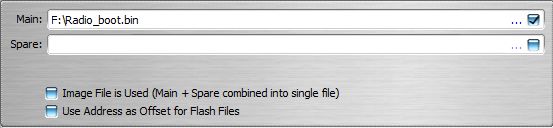
Selected file will be opened in Main field and used in flash write operations:
Spare data file field:
Used only for NAND flash memory type. All RIFF NAND files have both main and spare data combined into single file, so this field is to be used only in case that You have Your own Spare data file. With usual RIFF operations this field is NOT USED ! ! !
Option check boxes:
- Image file is used (Main + Spare combined into single file)
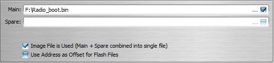
This option is to be used only with NAND files, previously read from working device. Only RIFF files are valid !
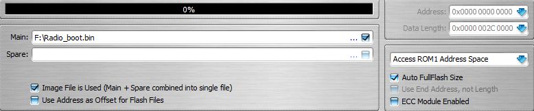
In above sample "Radio_boot.bin" file contains both main and spare data, combined into single file.
- Use address as Offset for Flash Files
This option is to be used in case that You need to write specific address range from full or partial flash image. For example, You have full flash image, and You want to write range from 0x000 0020 0000 and length 0x0000 0001 0000 to target device. This way You can "clone" sectors from one device to another, without waste of time by flashing full flash image.
For any Read/Write/Erase operation, starting address and data length must be supplied.
Address field value is used as starting address, and Data Length field value determines size. Both fields use hex format, devided into groups of four digits, for easier handling.
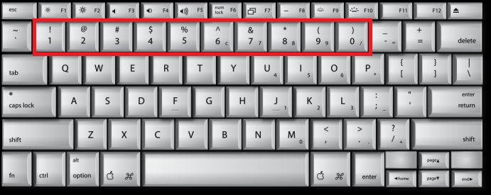
To enter start address, type the value into its field, using numeric keys on keyboard:
Data Length field can be used in multiple ways:
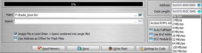
- File size:
Once You open file You want to use, and in case that You want to write whole file, simply select "File Size" from drop down menu. File size will be automagically read and inserted in Data Length field.
In this case, correct sequence should be: Open File -> Enter Address -> Select "File Size" from list.
- Pre-Defined size from list:
Clicking to blue arrow will bring list with pre-defined size. You can select any range from 1MB to 16GB.
- Manually entered value
Simply enter desired value using numeric keys on keyboard.
- Address Space
Used to select target device address space. In most devices, there is more internal address space ranges. Those can be devided into two basic groups:
- MCU Address space
- ROM Address space
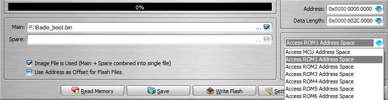
MCU Address space is internal CPU ROM, and as such it's read only. Furthermore, in many CPU-s access to this address space is restricted or blocked. For average user, this address space is of no use.
- ROM Address space
This is most important address space in practical use. Since many devices can have more then one phisycal flash memory chip, or, in case of eMMC more than one partition, they can be accessed by selecting different ROM number.
Most important if, of course, ROM1 address space, and it's main memory address space in all devices.
It's possible to select total of 8 ROM address spaces in RIFF JTAG Manager.
Optional settings:
- Autofull flash size
This option is used to automatically read flash chip size and apply values to address and length fields. When this option is checked, it disables address, data length fields, and "Use end address" option.
- Use end address, Not Length
This option is used instead of data length. Basically it does the same job, just instead of size, end address is provided.
- ECC Module enabled
This option is to be used only with NAND memory chips. It's function is to enable DCC loader to generate NAND spare data. RIFF files have already spare data included, so this option is not required with RIFF files. It should be used only in case where file contains only main data, and no spare. For example, data extracted from firmware files.
Read Memory button
Used to execute "Read" command, once required parameters are set. (Address, Length, Address Space)
Save button
Used to execute "Save" command, once read operation is finished successfully. It will open "Save File" dialog, where user can enter file name and select save location.
Erase Flash/Write Flash button
It's placeholder can change value, from Erase Flash to Write Flash. This depends on Main file check box:
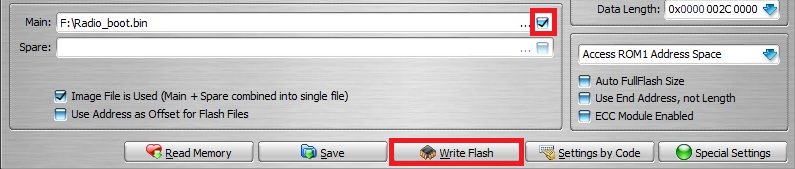
When Main file field check box is checked, this button transforms into "Write Flash", and it's used to execute "Write" Command.
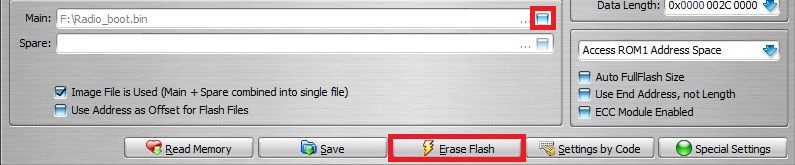
When Main file field check box is un-checked, this button transforms into "Erase Flash", and it's used to execute "Erase" command. Tricky, huh ?
WARNING ! ! !
DO NOT use "Erase" function with eMMC chips ! ! !
DO NOT use "Erase" function with eMMC chips ! ! !
Settings by Code button
Used to apply pre-defined preset from already defined settings options, or from settings code. Once clicked, it brings this menu, with two main options:
- Apply Pre-Defined Preset
- Apply settings from Settings Code
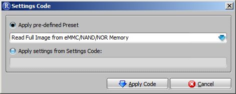
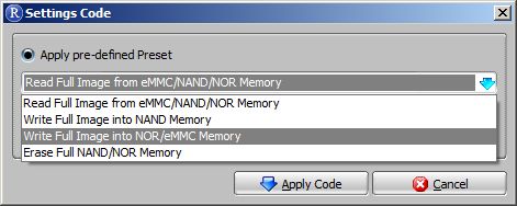
There are total four pre-defined presets:
- Read Full image from eMMC/NAND/NOR memory
- Write Full image into NAND memory
- Write Full image into NOR/eMMC memory
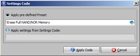
- Erase Full NAND/NOR memory
Pre-defined preset is used to automatically set correct all required settings and options.
Correct sequence to use this function is as follows:
Settings by code -> Select pre-defined preset -> Apply code -> Execute desired function.
Settings from Settings Code
Each time any operation is executed, settings code is generated, shown in log window and stored in log file. This code can be decoded into options and settings used for specific operation. We use it in case that users report some problems, to diagnose if user made some mistake in settings and options.
This code can be applied to new session, thus making life easier for RIFF users.
To read full flash image from target device, correct options must be set first. Easiest way is to use "Settings by code" button, following this sequence:
Settings by Code -> Select "Read Full Image from NAND/NOR/eMMC Memory" preset ->Apply Code -> Read Memory.
After this step, all required options and settings will be correctly set-up:
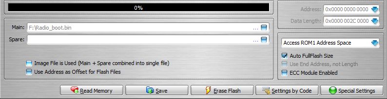
As You can see, ROM1 address space and Auto Fullflash size options is selected. Other options are irrelevant for read memory functions.
Once reading is finished, simply click "Save" button to save the file.
To write full flash image to target device, correct options must be set first. Easiest way is to use "Settings by code" button, following this sequence:
Open desired file -> Settings by Code -> Select Preset (Write NAND or NOR/eMMC) -> Apply Settings -> Write Flash.
If You are not sure which type of memory chip to select, here are some hints:
If You are not sure which type of memory chip to select, here are some hints:
- Most CDMA phones use NOR flash chip type
- Most older GSM/UMTS phones and USB modems use NAND flash chip type
- Most new GSM/UMTS phones use eMMC flash chip type
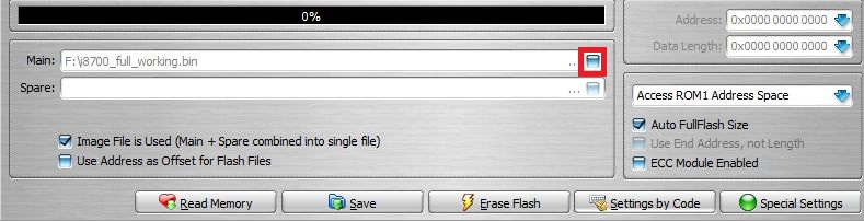
Final settings for NOR/eMMC memory will be like on bellow screenshot:
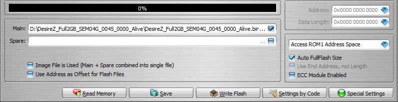
Important options and settings are ROM1 Address space, Auto FullFlash Size. All other options are irrelevant.
Final settings for NAND memory will be like on bellow screenshot:
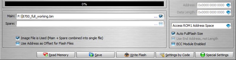
Important settings and options are ROM1 Address Space, Auto FullFlash Image and Image File is Used. ECC Module option MUST BE DISABLED ! ! !
To erase full flash image on target device, correct options must be set first. Easiest way is to use "Settings by code" button, following this sequence:
Settings by Code -> Select Erase Full NAND/NOR memory -> Apply Code -> Erase Flash.
Main file check box will be unchecked (in case that there is some file opened), ROM1 Address Space selected, and "Auto FullFlash size" option checked:
WARNING ! ! !
DO NOT use "Erase" function with eMMC chips ! ! !
DO NOT use "Erase" function with eMMC chips ! ! !
Erasing of eMMC memory chip is intentionally disabled. Due to specific eMMC memory architecture and data structure, erasing any part of it can cause more damage than good. This is why, even if erase function is executed, actually no data will be erased, but there can be some unpredicted results, like eMMC firmware lockup due to bugs in eMMC firmwares ! ! !